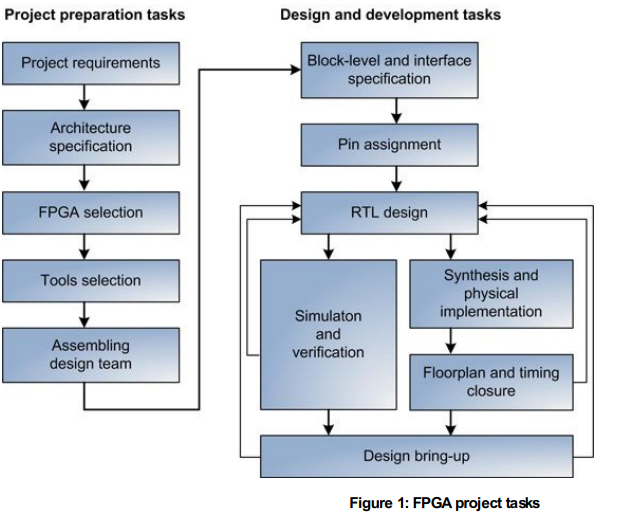
How your VHDL code becomes FPGA hardware: synthesis, implementation, and bitstream.
The Complete Design Flow
Step 1: Synthesis
Synthesis translates your VHDL into a network of logic gates (netlist).
What the synthesizer does
VHDL Construct
Inferred Hardware
AND, OR, NOT
Logic gates in LUTs
if rising_edge(i_clk)
D flip-flop
case on signal
MUX or LUT
array of signals
Registers or BRAM
* (multiplication)
DSP or LUTs
when/select
MUX
Example
-- VHDL codeo_y <= (i_a AND i_b) OR (
NOT
i_c);
Will be synthesized into a LUT-3 with the appropriate truth table.
-- VHDL codeprocess(i_clk)begin if rising_edge(i_clk) then r_data <= i_data; end if;end process;
Will be synthesized into a D flip-flop with i_data on the D input and r_data on Q.
Step 2: Technology Mapping
The abstract netlist is mapped onto the FPGA's physical resources.
The synthesizer chooses to use:
LUTs for combinational logic
D flip-flops for registered logic
BRAM for memories (if size is sufficient)
DSPs for multiplications
You can influence these choices with synthesis attributes:
-- Force to BRAM (Xilinx)attribute ram_style : string;attribute ram_style of r_mem : signal is "block";-- Force to distributed registersattribute ram_style of r_mem : signal is "distributed";
Step 3: Placement
Logic resources are assigned to physical locations on the FPGA.
Placement influences:
Maximum frequency (long signals = slower)
Power consumption
Resource utilization
You can constrain placement for timing reasons:
# Placement constraint (Xilinx XDC)set_property LOC SLICE_X0Y0 [get_cells r_counter_reg[0]]
Step 4: Routing
Interconnects between placed resources are configured.
Routing is often the timing bottleneck. Signals traversing many interconnect resources introduce delays.
Static Timing Analysis (STA)
The tool performs static timing analysis to verify that all paths meet constraints.