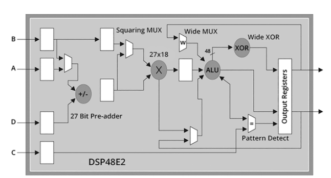
FPGA Internal Architecture
LUTs, flip-flops, block RAM, DSP, interconnects - the physical resources of a modern FPGA.
What is an FPGA?
An FPGA (Field-Programmable Gate Array) is an integrated circuit whose logic is reconfigurable after manufacturing. Unlike an ASIC (fixed circuit), an FPGA can be reprogrammed as many times as needed.
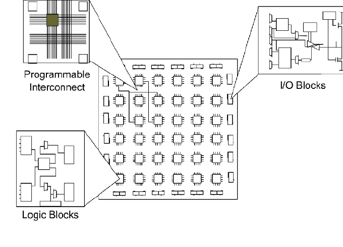
Main Resources
LUT - Look-Up Table
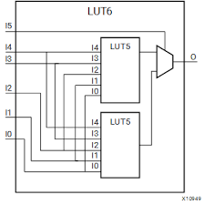
The basic building block of configurable logic. A LUT is a small memory that implements any logic function.
A LUT-6 (6 inputs, standard Xilinx 7-series) can implement any function of 6 variables → 2⁶ = 64 memory locations.
| Parameter | Xilinx 7-series | Intel Cyclone V |
|---|---|---|
| LUT | LUT-6 | LUT-6 (ALM) |
| LUTs / CLB | 8 | 10 / ALM |
| Typical count | 13k – 2M | 25k – 300k |
D Flip-Flop
Each LUT is paired with one or more D flip-flops. They store state between clock cycles.
A CLB (Configurable Logic Block) typically contains 8 LUTs + 16 flip-flops.
Carry Chain
CLBs have fast carry propagation chains, enabling high-performance adders and counters.
BRAM - Block RAM
On-chip memory embedded in the FPGA. Organized in fixed-size blocks (typically 18 kbits or 36 kbits).
-- Simple-port BRAM automatic inference
architecture rtl of bram_sp is
  type t_mem is array(0 to 255) of std_logic_vector(7 downto 0);
  signal r_mem : t_mem;
begin
  process